PCB Viewer
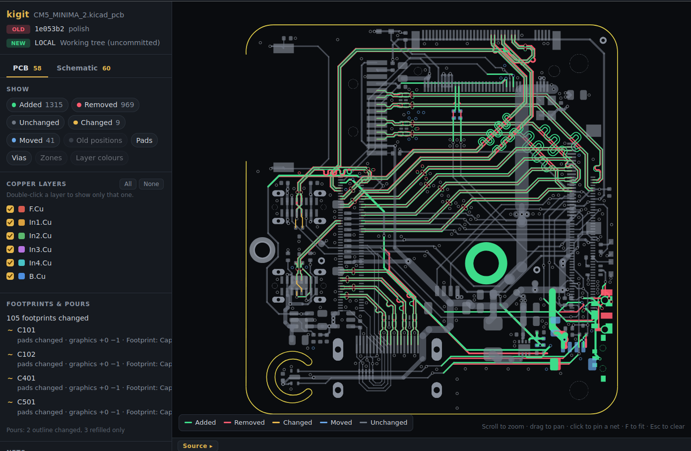
The PCB tab draws both revisions of the board on top of each other.
| Action | What it does |
|---|---|
| Hover a trace, via or pad | Highlight its net, show the net's changes |
| Click | Pin the net (click again or Esc to clear) |
| Scroll / drag | Zoom / pan |
F |
Fit the board |
/ |
Filter nets |
| Double-click a net in the list | Zoom to it |
How items are matched
Tracks, arcs, vias and pads are matched in two passes:
- By KiCad's ID (the ID KiCad gives every item and keeps when you move it; a pad uses its footprint's ID plus its pad number). Same ID and same place: unchanged. Same ID and same copper at a new place or angle: moved, shown in blue, with an optional ghost at the old position. Same ID but edited (a dragged track end, a new width or net): removed + added.
- By geometry for everything else: same kind, net, layers and coordinates (to 1 nm) means unchanged.
So moving a footprint or the whole layout shows as moved, not as everything removed and re-added, while re-routing still shows the new and old copper.
Silkscreen
Off by default (--silkscreen, or "Include silkscreen" in the GUI) since it makes pages bigger. Front silkscreen is drawn near-white, back purple and mirrored, each with its own layer toggle. Text uses a browser font, so it's close to KiCad's but not identical.
Zones
Copper pours are drawn from the newer revision only and aren't diffed, because refilling a pour changes its shape every time.