Schematic Viewer
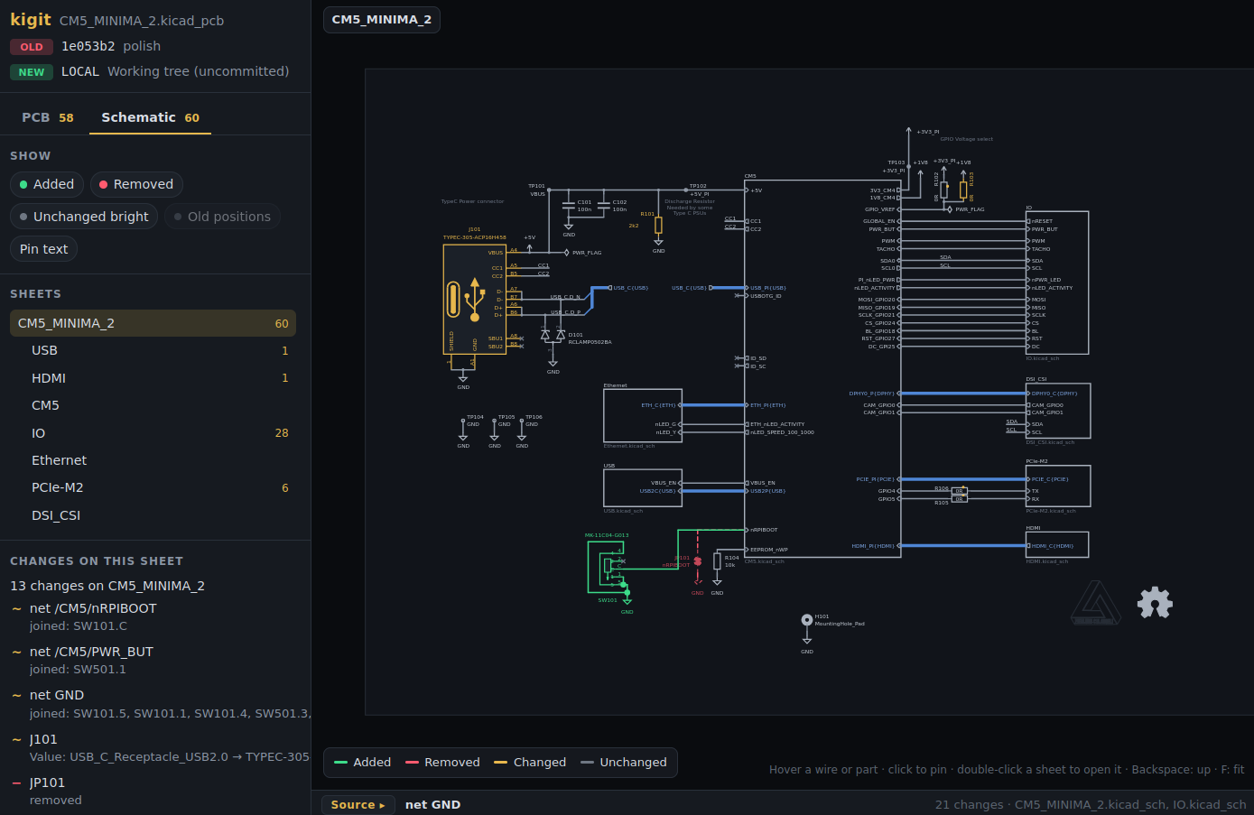
The Schematic tab draws each sheet (wires, parts, labels, sheet boxes) with the same colours as the PCB: green added, red dashed removed, amber for parts whose value, footprint or connections changed, grey unchanged.
| Action | What it does |
|---|---|
| Hover a wire, label or pin | Highlight its net; the tooltip shows pins that joined or left, renames, or "wiring redrawn, connections unchanged" |
| Hover a part | Its changes: fields (value, footprint, MPN...), pins moved to other nets, moved |
| Click | Pin it; the card can jump to other sheets the net is on |
| Double-click a sheet box | Open that sheet (Backspace goes back up) |
| Sidebar | Sheet tree with change counts, and the changes on the current sheet |
"Old positions" shows moved parts' previous place as a faint ghost (off by default).
Nets
kigit works out the schematic's nets itself, across all sheets, buses (D[0..7], groups, aliases like USB_C{USB}) and KiCad 10's multiple top-level sheets. You can check them against KiCad's own netlist:
In the terminal
Every run also prints the schematic changes:
schematic: parts +1 -0, 8 changed electrically, 1 fields only, 0 only moved; 3 nets changed, 0 renamed, 1 only redrawn
  ~ J3     J3.1 (Pin_1): /owl_v1/CAN Transceiver/CAN_H -> GND, moved
  + R19    R          [IOs] on +3.3V, GND
  ~ C14    Footprint Capacitor_SMD:C_0402_1005Metric -> Capacitor_SMD:C_0603_1608Metric
  ~ net GND                      joined: J3.1 (Pin_1), R19.2  left: J3.3 (Pin_3)
Note
The drawing is kigit's own, not KiCad's export: close to KiCad but with a different font, and images and text boxes aren't drawn yet.